Ch9
Ch9
整数表示法
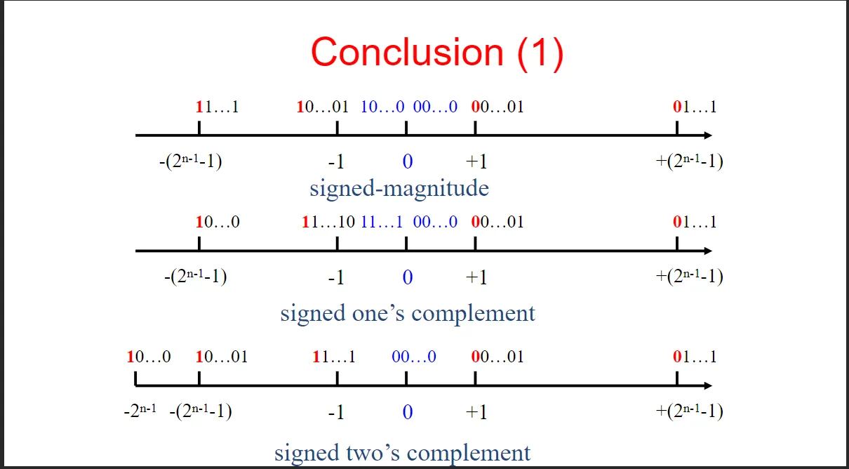
原码表示法(Signed-Magnitude Representation),反码表示法(Signed One’s Complement Representation)和补码表示法(Signed Two’s Complement Representation)。
一个n位比特数,最低位是第 0
位,最高位是n-1位,可以表示的范围是从\(0\)~\(2^n-1\)。
原码表示法(Signed-Magnitude Representation)
符号位是最高位,0 表示正数,1 表示负数。
剩下n-1位表示的是这个数字的绝对值。
原码表示的范围:
\[ -(2^{n-1}-1) \leq V(B) \leq 2^{n-1}-1 \]
原码表示法简单易理解,但是加法和减法需要考虑数字的符号及其相对大小以执行所需的操作– 0 有两种表示形式,不方便处理。
反码表示法(Signed One’s Complement Representation)
符号位是最高位,0 表示正数,1 表示负数。
正数:相当于有符号正整数的整数部分。
负数:对应的正数每一位取反。
补码表示法(Signed Two’s Complement Representation)
符号位是最高位,0 表示正数,1 表示负数。
正数:相当于有符号正整数的整数部分。
负数:对应的正数每一位取反,再加一。
补码表示的范围:
\[ -2^{n-1} \leq V(B) \leq 2^{n-1}-1 \]
不同位长之间进行转换
原码
将符号位移动到新的最左侧位置并用零填充。
+18 = 00010010 (8 位) |
补码
如果按照上面的做法:
+18 = 00010010 (8 位) |
这里采取这种做法:将符号位移动到最左侧的新位置,并填写符号位的副本。对于正数,请填写 0,对于负数,请填写 1。
-18 = 11101110(8 位) |
整数运算
算术溢出:算术运算的结果超出可表示范围。
充分和必要的条件:如果两个数字相加,并且它们具有相同的符号,则当且仅当结果与两个求和的符号相反时,才会发生溢出。
注意:添加有符号数字时,来自符号位位置的 carry-out 信号不足以表示溢出。无论是否有结转,都可能发生溢出。
减法运算:将减数作为一个负数处理(原来的正数取反加一得到),然后执行加法即可。
行波进位加法器和加法/减法单元
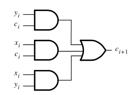
1 位全加器
A full adder circuit takes three bits of input, and produces a two-bit output consisting of a sum and a carry out.
全加法器电路采用 3 位输入,并产生由 sum 和 carry 组成的 2 位输出。
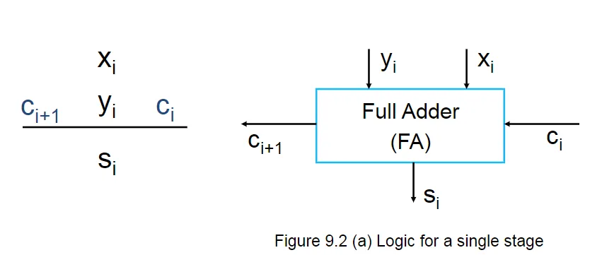
其中\(s_i\)和\(c_{i+1}\)的组成分别如下:
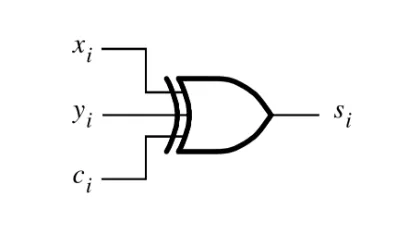
\[ s_i=x_i \oplus y_i \oplus z_i \]
\[ c_{i+1}=y_ic_i+c_ix_i+x_iy_i \]
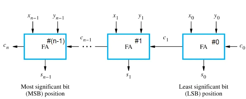
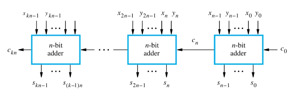
n 位行波加法器
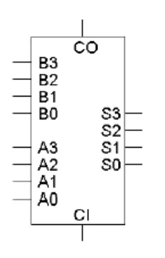
先由一个 4 位的加法器进行引入:
四个全加法器一起构成一个 4 位加法器。总共有九个输入:
- 两个 4
位数字,
A3 A2 A1 A0和B3 B2 B1 B0。 - 初始进位
CI
另外有五个输出:
一个 4 位和:
S3 S2 S1 S0一个进位输出:CO
简单电路图
内部结构图
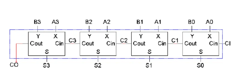
由此我们可以推广到n位。
我们还需要考虑计算溢出的情况:
这里之前提到:只有两个数字的最高符号位与计算结果的符号位不同时,才是溢出。利用这个性质,可以得到计算是否溢出的逻辑表达式:
\[ Overflow=x_{n-1}y_{n-1}\bar s_{n-1} + \bar x_{n-1}\bar y_{n-1}s_{n-1} \]
还可以利用:
\[ Overflow=c_n \oplus c_{n-1} \]
来判断是否溢出。
分层加法器(Hierarchical Adder)
我们可以通过将若干个n位加法器进行串联,从而得到kn位加法器。
门延迟
这里假设所有的门的延迟都是相同的。
The delay through a network of logic gates depends on the integrated circuit electronic technology used in fabricating the network and on the number of gates in the paths from inputs to outputs.
The delay through any combinational logic network constructed from gates in a particular technology is determined by adding up the number of logic-gate delays along the longest signal propagation path through the network
在n位行波加法器中,最长的路径就是从 LSB 位置的\(x_0,y_0,z_0\)到 MSB 的\(c_n\)和\(s_{n-1}\)。
我们假设每个逻辑门的延迟都是 T,那么\(delay(s_i)=T,delay(c_{i+1})=2T\)。(联系上面的电路图)
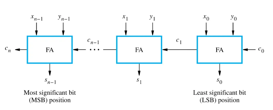
我们可以由此计算出\(c_{n-1}=2(n-1)T\),\(s_{n-1}=2(n-1)T+T=(2n-1)T\),\(c_n=(2n)T\)。
加分和减法逻辑单元
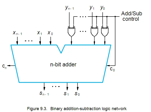
这里主要是利用了异或的运算规则:$0 Y=Y,1Y= Y $。
当 Add/Sub control 为 0 时,执行加法,所有数不变。
当 Add/Sub control 为 1
时,执行减法,y所有位数取反,并且\(c_0\)为 1,恰好实现到补码的转换。
All sum bits are available in 2n gate delays, including the delay through the XOR gate on the Y input.
更快加法器的设计
n位行波加法器的延迟太多了,所以探索进一步的优化。
生成函数和传播函数(Generate Function and Propagate Function)
\[ s_i=x_i \oplus y_i \oplus z_i \\ c_{i+1}=y_ic_i+c_ix_i+x_iy_i \\ G_i=x_iy_i(generate \ function \ for \ stage \ i)\\ P_i=x_i+y_i(propagate \ function \ for \ stage \ i)\\ c_i=G_i+P_ic_i \]
我们研究能否进行一些门的替换: \(P_i=x_i+y_i \rightarrow P_i=x_i \oplus y_i\)
可以发现除了\(x_i=y_i=1\)的情况外,其余情况下\(P_i\)的值都是相同的,并且此时\(G_i=1\),\(c_i\)必为 1。
所以可以将\(P_i=x_i+y_i \rightarrow P_i=x_i \oplus y_i\)。
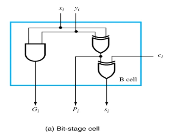
可以得到的逻辑表达式如下:
\[ c_{i+1}=G_i+P_ic_i\\ =G_i+P_i(G_{i-1}+P_{i-1}c_{i-1})\\ =···\\ =G_i+P_iG_{i-1}+P_iP_{i-1}G_{i-2}+···+P_iP_{i-1}···P_1G_0+P_iP_{i-1}···P_0c_0 \]
All carries can be obtained 3 gate delays after the input signal X, Y and c0 are applied.
All sum bits are available 4 gate delays after the input signal X, Y and c0 are applied.
所有进位门的延迟都是 3,所有sum的延迟是
4。(注意前者是指单个门,后者是指整个结果)。
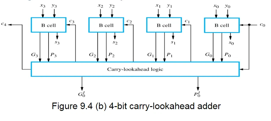
The 4-bit carry-lookahead adder design cannot be directly extended to longer operand sizes
这里是因为 Fan-In 约束的限制。
Fan-in: The number of inputs to a logic gate is called its fan-in
Fan-out: The number of gate inputs that the output of a logic gate drives is called its fan-out
Practical circuits do not allow large fan-in and fan-out because they both have an adverse effect on the propagation delay and hence the speed of the circuit.
实际电路不允许大的扇入和扇出,因为它们都对传播延迟有不利影响,从而对电路的速度产生不利影响
Fan-in of the last AND gate and the OR gate is i+2 in generating \(c_{i+1}\).(联系逻辑表达式)
所以后续采用串联的方法,构成更长位数的加法器。
以用 4 位加法器构建 32 位加法器为例:
Calculate the delays in generating sum bits \(s_{28}\), \(s_{29}\), \(s_{30}\),\(s_{31}\),and \(c_{32}\) in the high-order 4-bit adder.
| \(c_4\) | 3T |
|---|---|
| \(c_8\) | 3T+2T=5T |
| \(c_{12}\) | 5T+2T=7T |
| \(c_{28}\) | (2·7+1)T=15T |
| \(c_{29},c_{30},c_{31},c_{32}\) | 17T |
| \(s_{28}\) | 16T |
| \(s_{29},s_{30},s_{31}\) | 17T+T=18T |
这里是因为最初的\(x,y\)都是同时输入的(所以内部的计算\(P\)和\(G\)不用再考虑)只需要考虑进位\(c_{i+1}\)表达式的与门和或门的计算即可。
无符号数乘法
手动乘法算法(Manual Multiplication Algorithm)
Multiplication of the multiplicand by one bit of the multiplier(被乘数乘以乘数的一位) – If the multiplier bit is 1, the multiplicand is entered in the appropriate position.
(如果乘法器位为 1,则在适当的位置输入被乘数。如果乘数位为 0,则输入 0。) – If the multiplier bit is 0, then 0s are entered.
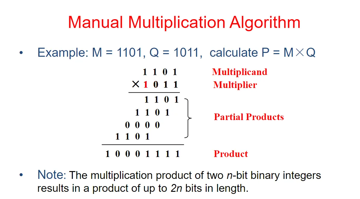
注意:两个n位二进制整数的乘积产生长度高达2n位的乘积。
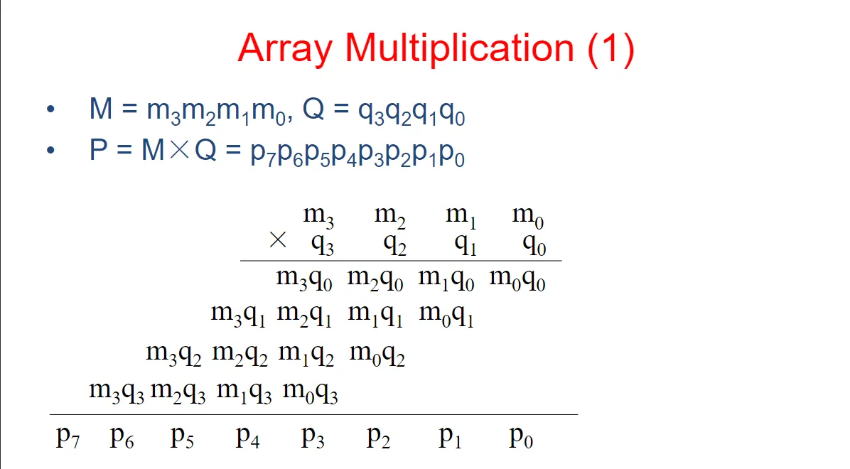
阵列乘法(Array Multiplication)
我们根据上述过程,进行一般化的模拟。
再看一下硬件是如何实现的:
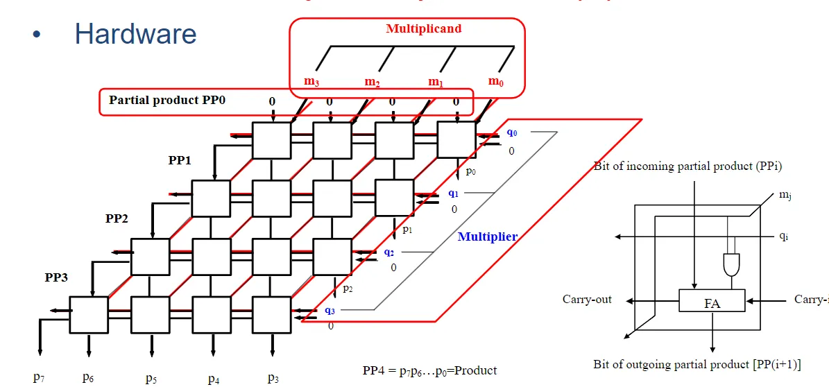
注意看每个小方阵:里面是一个 AND 门和一个一位加法器。
由于涉及到多个数相加,所以我们可以利用累加的方法进行实现(这里由FA一位加法器进行实现)。
另外根据原理,\(m_i\)需要从上向下传递,\(q_i\)需要从右到左传递,所以能看到一条电路线直接贯穿(没有发生任何修改)。
同时还需要注意到:输出进位对累加的结果也会有影响,所以最高位的输出进位也需要进行累加。
接下来计算:
When calculating P = M × Q (M and Q are all n bit unsigned binary numbers) , how many FAs and AND gates do we need (using n×n array multiplier)?
我们可以发现最初两个值相加:其中一个是
0,所以不需要考虑上面的数字对当前累加计算的影响。所以最顶层可以不用FA。
由图可得:
FAs:\(n(n-1)\)
AND gates:\(n^2\)
顺序乘法(Sequential Multiplication)
Multiplication of two n-bit numbers can also be performed in a sequential circuit that uses a single n-bit adder
两个
n位数的乘法也可以在使用单个n位加法器的sequential circuit中执行。
这个的实现具体原理稍复杂,先给出硬件图片:
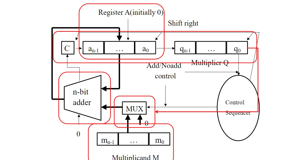
这里是通过右移动实现的,假设我们只有n位的寄存器。
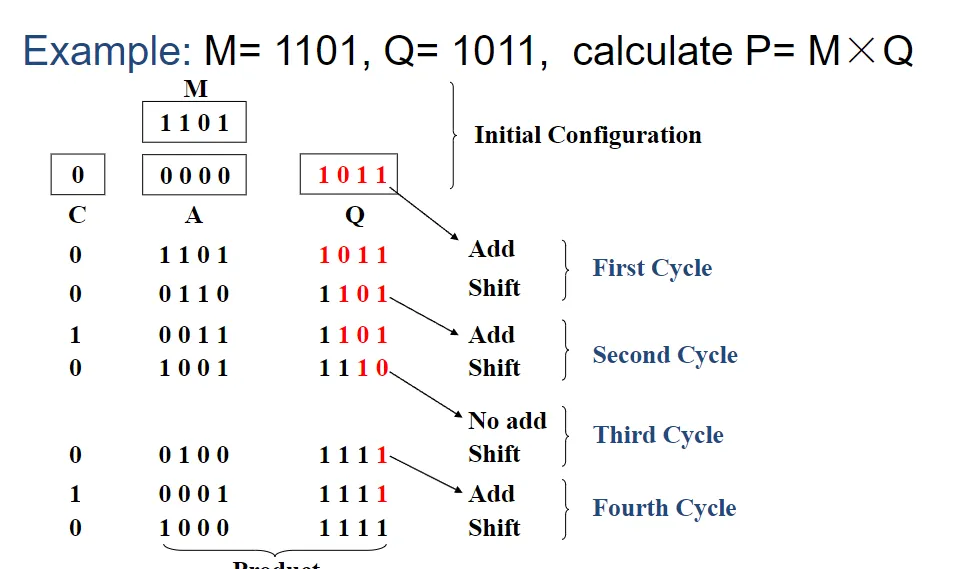
利用下面图中的这个例子:
如果是老方法,那么肯定2nd Partial Products肯定会丢去最高位,那么我们可以怎么办?
我们可以右移:没执行一次乘法后,就右移一位,这样就解决了这个问题。
但是原来右移后的位数(作为结果的一部分)不见了。怎么办?
我们发现Q的最低一位也没有用了,实际上就只有三位有用。那么我们就可以右移Q一位,多出来的空白位就用来存储。
另外还是需要一个进行累加计算的寄存器(对应的就是硬件图中的a,C代表的是进位),由于一直右移,所以实际上影响运算的只有\(q_0\),我们可以使用一个多路复用器mux:如果是
1,进行累加,如果是 0,直接加 0。
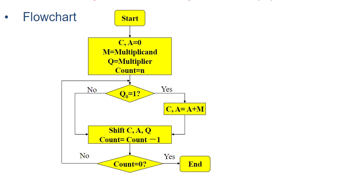
具体的执行流程图如下:
一道对应的例题:加深理解。
有符号数乘法(Multiplication of Signed Numbers)
Booth 算法
算法原理
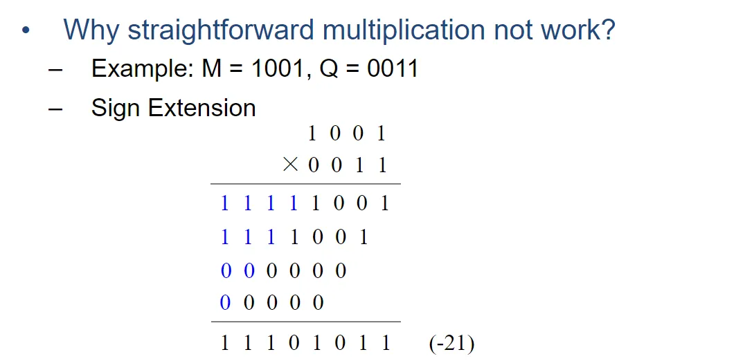
Straightforward multiplication will not work in the case of a negative operand or two negative operands
直接乘法在一个负操作数或两个负操作数的情况下不起作用。(可以看看下面的例子)。
针对有符号数乘法,比较常见的想法是:转换为无符号,进行乘法,然后转换回有符号。但是速度慢且麻烦。
这里引入Booth算法:可以直接处理有符号数字的乘法运算
- Recodes the bits of the multiplier(重新编码乘数的位)
- Works with 2’s complement numbers directly(直接处理补码)。
Booth算法的核心是:
Reducing number of partial products, Fewer partial products generated for groups of consecutive 0’s and 1’s. 即减少连续 1 的个数。
Group of consecutive 0’s in multiplier – no new partial product – only shift partial product right one bit position for every 0.
乘数中的一组连续 0, 没有产生新的部分乘积,仅每次遇到 0 将部分乘积,右移一位。
Group of m consecutive 1's in multiplier – less than m partial products generated
乘数中 m 个连续的 1 组,生成的部分乘积少于 m 个。
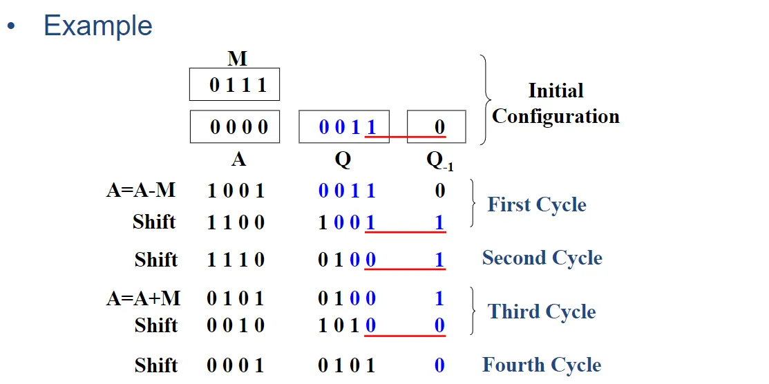
一个例子:能够很好的说明Booth算法的编码机制。
Example: 0011110 = 0100000 – 0000010 (decimal notation: 30 = 32 – 2)
可以发现:可以表示成两个数的加法,其中一位进 1,另外一位是原来的最低位。
更一般的原理如下图(上面是课本的原理,下面是比较简单的方法,也是例子)
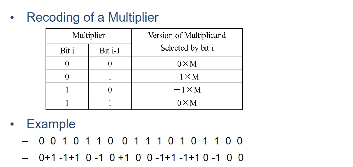
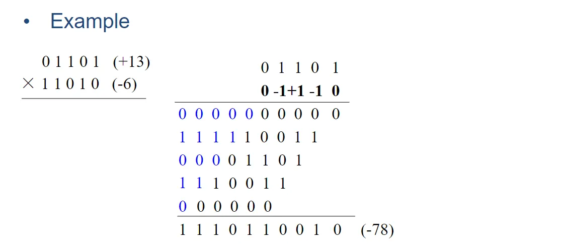
那么按照这种方法,我们进行实际操作一下:
011010 进行变换:(这里最高位前面先补充一位,所以就是 011010)+1 0 -1 +1 -1 0。
后续进行常规的乘法计算。(注意当是-1时,进行的是算术右移,也就是新填充的位是根据原来的最高位)。
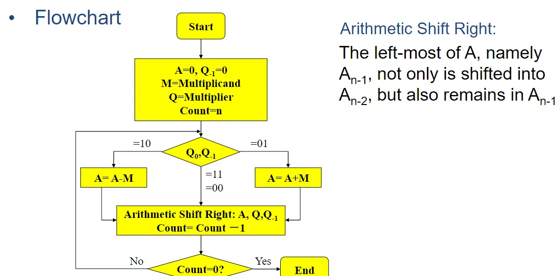
硬件组织
As before, the multiplicand and multiplier are placed in the M and Q registers, respectively
和以前一样,被乘数和乘法器分别放在 M 和 Q 寄存器中。
There is a 1-bit register placed logically to the right of the least significant bit (\(Q_0\)) of the Q register and designated \(Q_{-1}\)
有一个 1 位寄存器在逻辑上放置在 \(Q_0\) 寄存器的最低有效位 (\(Q_1\)) 的右侧,并指定为 \(Q_0\)
Control logic scans the bits of the multiplier one at a time. Now, as each bit is examined, the bit to its right is also examined
The results of the multiplication will appear in the A and Q registers.
流程图见下:
实际例子,配合学习效果更佳。